| Hy-Star ☆ Tech Support |

![]()
八核心平行處理單晶片 (FPPA) 介紹
Frank Chen
HY-STAR TECHNOLOGY CO.,LTD
引用或複製請註明出處
八核心平行處理單晶片 (FPPA) 介紹
相信許多研發人員都有選擇 MCU 的痛苦經驗, 選這顆 MCU 少個 UART,選那顆 Timer 又不夠,就算選好了 MCU,寫多功 (Muti-Task)的軟體才是真正痛苦的開始.
應廣科技 (Padauk )八核心平行處理單晶片 Field Programmable Processor Array,
以下簡稱 “FPPA”,利用八核心平行處理可一次解決軟體“Muti-Task” ,“Timer” 和 MCU 所需的各種周邊的困擾.有八顆
MCU 平行處理,不用再煩惱多工軟體,有八顆 MCU 平行處理等於有八個 Timer,不用再煩惱 Timer 不夠,有八顆 MCU
平行處理,拿幾顆來寫 UART,I2C,SPI,PWM 等周邊就不用再煩惱介面不夠.

如上圖所示
- 基本上應廣科技 (Padauk )的 FPPA, inside 了8 顆 RISC type 1T 的 MCU, 除了每顆 MCU 有自己的 Flag ,PC counter, Stack pointer, Accumulator 外,其餘的 ROM,RAM,IO 等是共用的.故每一 MCU 都可隨時監控其他 MCU 的狀況.(MCU#0 還多了 16bit 的 timer & 中斷管理可處理 I/O中斷和內部中斷).
- 8 顆 MCU 是平行處理,且每個 I/O 都可設為 input 或 output 或 pull-hi 或 open-drain,故可用軟體去控制 I/O寫各種周邊介面, 如 I2C, UART,PWM,SPI 等非常有彈性 (如 MCU#0 寫 UART, MCU#1寫 I2C, MCU#2 寫 PWM 等,幾乎沒有限制.) 軟體去作 SOC 周邊功能,故成本很有競爭力,和彈性,不會受限一般 MCU 原廠所開的 IC 規格.
- 除了 一般 MCU 的指令外, 還有 類似 FPGA 才有 I/O 指令,對 I/O 的處理特別精簡和有效率.可取代部分的 PAL/GAL/FPAG 等邏輯合成電路.
- 內建 8 顆 RISC type 平行處理,多核心 CPU 矩陣 (Field Programmable Processor Array“FPPA”).
- 內建硬體的即時作業系統 (hardware RTOS).
- 97 個 1T RISC type 功能強大的指令. (不同系列,指令略有增減)
- 支援 C/Assembly language/Macro 程式語言.
- 可自由規劃每一 MCU 的堆疊(stack pointer) 深度.
- 支援12bitx8ch ADC.
- 彈性方便的位元操作指令 (Bit-manipulation).
- 全部的資料記憶體都可用指標定址 (index pointer addressing).
- 可自由規劃每一 MCU 的程式空間 ( OTP program memory).
- 每一 I/O 都可彈性定義為 input 或 output或 pull-hi或 open-drain.
- 內建高速/慢速 RC振盪器.
- 獨家的 intra-FPP handshaking指令,每一 MCU 可控制其他 MCU 的程式指標 (program counter).
- 獨家的內部中斷,MCU#1 – MCU7 可發出中斷需求,讓 MCU#0當中斷優先處理.
- 獨家的 “wait0”, “wait1” 指令,對 IO 的處理特別精簡和有效率.
- 獨家的 “delay x” (x form 0 – 255)指令,可直接 delay x 的 system clock.
FPPA 最多可有 8 顆 MCU 同時平行處理, FPPA 有一“pmode”指令可調整每一 MCU 的速度,FPPA 根據“pmode”由硬體強制去分配的每一 MCU 的 bandwidth 來完成類似軟體 RTOS 的功能
(如下表),完全不用寫軟體的 RTOS.
| pmode | FPP0 | FPP1 | FPP2 | FPP3 | FPP4 | FPP5 | FPP6 | FPP7 |
| 0 | 1/2 | 1/8 | 1/16 | 1/16 | 1/16 | 1/16 | 1/16 | 1/16 |
| 1 | 1/4 | 1/4 | 1/8 | 1/8 | 1/16 | 1/16 | 1/16 | 1/16 |
| 2 | 1/8 | 1/8 | 1/8 | 1/8 | 1/8 | 1/8 | 1/8 | 1/8 |
| 3 | 1/2 | 1/8 | 1/8 | 1/8 | ||||
| 4 | 1/4 | 1/4 | 1/4 | 1/8 | 1/8 | |||
| 5 | 1/16 | 1/4 | 1/4 | 1/4 | 1/16 | 1/16 | 1/16 | |
| 6 | 1/16 | 1/2 | 1/8 | 1/16 | 1/16 | 1/16 | 1/16 | 1/16 |
| 7 | 1/8 | 1/2 | 1/8 | 1/8 | 1/8 |
如下圖為 pmode =2 , 平均每一 MCU 分配 1/8 system clock
 <pmode =2>
下圖為 pmode=0 ,FPP#0 = 1/2 system clock, FPP#1 = 1/4 system clock, FPP#2-FPP#7 = 1/16 system clock ,每個 FPP 的 cycle 如下
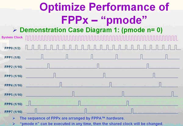 <pmode=0>
|
PPA 共有 33 個暫存器(不同系列暫存器略有不同),其中 address 0x10 – 0x32 各為 I/O Port A – Port E 的控制暫存器,故真正要注意的 register 只有 13 個,不像其他 MCU,周邊控制 (如PWM,I2C,UART 等)的 register 就好幾拾個,故 FPPA 很容易學習U. 13個 register 中比較容易引起誤解,或 datasheet 描述不易理解的地方特別提出說明.
- “sp” & “flag”: 由於 FPPA 有8顆 MCU,故每一 MCU 看到的 “sp” & “flag” 的值是不一樣的值.
- “fppen”: 由於 FPPA 有8顆 MCU,但並不是每個應用 8 顆 MCU 都要去 enable, 故可用 “fppen” register 去控制那些 MCU 需要 enable.
- gdio”: register “gdio” 可以做下列二種應用
- 當 warm-boot 或 cool-boot的判斷用:由於 FPPA 開機或 reset 時, “gdio” 的值不會去變更,故程式執行中可故意寫入一個值給 “gdio”,而在程式開始的地方去判斷 “gdio” 的值是否為程式執行中所寫入的值即可判斷 MCU 是否是第一次開機或是 reset 再開機.
- 讓 MCU & MCU 間的溝通更有效率:“wait0” 和“ wait1” 指令 除了可對 I/O 處理外, 也可對 “gdio” 暫存器處理, (Ex.: “wait0 gdio.x”), 例如在 MCU#1 中把“gdio.x” 設為 0 或 1, MCU#2 用 “wait0” 或 “wait1”指令去做條件的判斷亦可達到 MCU#1 和 MCU#2 之間的溝通.

如上圖所示,和大多數的 MCU 一樣,FPPA 也有所謂 “中斷向量表”的概念,只是一般 MCU 的中斷向量是“中斷副程式” 的進入位置,FPPA 的中斷向量是各 FPP 的進入位置.如上圖中 address 0h-7h 分別為 FPP#0-7 的進入位置,address 0x10 才是“中斷副程式” 的進入位置,故其程式寫法如下

| FPPA Instructions Set | |
| Data Transfer Instructions (16) | |
| Instruction | Function |
| mov a,I | Move immediate data to ACC。 |
| mov M,a | Move data from ACC to memory |
| mov a,M | Move data from memory to ACC |
| mov a,IO | Move data from IO to ACC |
| mov IO,a | Move data from ACC to IO |
| pushw index | Move the content of index to be the content of stack pointer |
| pushw pcN | Move the content of program counter of Nth FPP unit to be the content of stack pointer |
| popw index | Restore the content of stack pointer to be the content of index |
| popw pcN | Restore the content of stack pointer to be the content of program counter of the Nth FPP unit |
| ldtabh index | Load high byte data in OPT to ACC by using index as OPT address |
| ldtabl index | Load low byte data in OTP to ACC by using index as OTP address |
| ldt16 index | Move 16-bit counting values in Timer16 to memory which is addressed by index |
| stt16 index | Store 16-bit data from memory addressed by index to Timer16 |
| idxm a,index | Move data from specified memory to ACC by indirect method |
| idxm index,a | Move data form ACC to specified memory by indirect method |
| xch M | Exchange data between ACC and memory |
| Arithmetic Operation Instructin (20) | |
| add a,I | Add immediate data with ACC, then put result in ACC |
| add a,M | Add data in memory with ACC, then put result in ACC |
| add M,a | Add data in memory with ACC, then put result in ACC |
| addc a,M | Add data in memory with ACC and carry bit, then put result in ACC |
| addc M,a | Add data in memory with ACC and carry bit, then put result in memory |
| addc a | Add carry with ACC, then put result in ACC |
| addc M | Add carry with memory, then put result in memory |
| nadd a,M | Add negative logic (2's complement) of ACC with memory |
| nadd M,a | Add negative logic (2's complement) of memory with ACC |
| sub A,I | Subtraction immediate data from ACC, then put result in ACC. |
| sub a,M | Subtraction data in memory from ACC, then put result in ACC. |
| sub M,a | Subtraction data in ACC from memory, then put result in memory |
| subc a,M | Subtraction data in memory and carry from ACC, then put result in ACC |
| subc M,a | Subtraction ACC and carry bit from memory, then put result in memory |
| subc a | Subtraction carry from ACC, then put result in ACC |
| subc M | Subtraction carry from the content of memory, then put result in memory |
| inc M | increment the content of memory |
| dec M | Decrement the content of memory |
| clear M | Clear the content of memory |
| mul | Multiplication operation. An 8x8 unsigned multiplication will be executed. |
| Shift Operation Instructions (11) | |
| sr a | Shift right of ACC |
| src a | Shift right of ACC with carry |
| sr M | Shift right the content of memory |
| src M | Shift right of memory with carry |
| sl a | Shift left of ACC |
| slc a | shift left of ACC with carry |
| sl M | Shift left of memory |
| slc M | Shift left of memory with carry |
| swap a | Swap the high nibble and low nibble of ACC |
| swap M | Swap th high nibble and low nibble of memory |
| Logic Operation Instructions (16) | |
| and a,I | Perform logic AND on ACC and immediate data, then put result in ACC |
| and A,M | Perform logic AND on ACC and memory, then put result in ACC |
| and M,a | Perform logic AND on ACC and memory, then put result in memory |
| or a,I | Perform logic OR on ACC and immediate data, then put result in ACC |
| or a,M | Perform logic OR on ACC and memory, then put result in ACC |
| or M,a | Perform logic OR on ACC and memory, then put result in memory |
| xor a,I | Perform logic XOR on ACC and immediate data, then put result in ACC |
| xor a,M | Perform logic XOR on ACC and memory, then put result in ACC |
| xor M,a | Perform logic XOR on ACC and memory, then put result in memory |
| not a | Perform 1's complement (logical complement) of ACC |
| not Mry | Perform 1's complement (logical complement) of memo |
| neg a | Perform 2's complement of ACC |
| neg M | Perform 2's complement of memory |
| comp a,I | Compare ACC with immediate data |
| comp a,M | Compare ACC with the content of memory |
| comp M,a | Compare ACC with the content of memory |
| Operation Instructions (6) | |
| set0 IO.n | Set bit n of IO port to low |
| set1 IO.n | Set bit n of IO port to high |
| tog IO.n | Toggle bit state of bit n of IO port |
| set0 M.n | Set bit n of memory to low |
| set1 M.n | Set bit n of memory to high |
| swapc IO.n | Swap the n-th bit of IO port with carry bit |
| Conditonal Operation Instructions (13) | |
| ceqsn a,I | Compare ACC with immediate data and skip next instruction if both are equal |
| ceqsn a,M | Compare ACC with memory and skip next instruction if both are equal |
| cesn M,a | Compare ACC with memory and skip next instruction if both are equal |
| t0sn IO.n | Check IO bit and skip next instruction if it's low |
| t1sn IO.n | Check IO bit and skip next instruction if it's high |
| t0sn M,n | Check memory bit and skip next instruction if it's low |
| t1sn M,n | Check memory bit and skip next instruction if it's high |
| izsn a | increment ACC and skip next instruction if ACC is zero |
| dzsn a | Decrement ACC and skip next instruction if ACC is zero |
| izsn M | Increment memory and skip next instruction if memory is zero |
| dzsn M | Decrement memory and skip next instruction if memory is zero |
| wait0 IO.n | Go next instruction until bit n of IO power is low; otherwise, wait here |
| wait1 IO.n | Go next instruction until bit n of IO power is high; otherwise, wait here |
FPPA 共有97 個 (不同系列,指令略有增減)1T RISC type 功能強大的指令.大部分的指令看 datasheet 就知道其用法,不再多敘,這裡只介紹比較容易引起誤解,或 datasheet 敘述不容易理解的地方特別提出說明
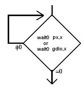
- wait0,wait1:
只能針對 I/O 或 register “gdio”,但不能對記憶體, 其功能如流程圖所示,一直要等到 I/O 或 gdio.x =0 或 1
成立才往下繼續執行,因傳統的 MCU,只有一顆 MCU,故無法去實現這種指令,否則如果條件不成立,程式就一直停在那,形同“當機”.

- delay :直接 delay x 個 system clock 才往下繼續執行, 例如 system clock = 8Mhz,pmode = 0,FPP#0 執行 “delay 100” =100*1/4M = 25us,但 FPPA#1執行“delay 100” = 100 * 1/1M = 100us.
- pushw,popw: push & pop 程式指標
由 於 PFPA 是一顆 8 核心的 MCU,不同 MCU 間可更改彼此的程式指標 “pc”, 來達到強迫其他 MCU 去執行某段程式的路徑之目的,但要小心運用,否則容易破壞程式的結構.下例中的 FPP#0 原本只會在 LOOP_A無窮的回圈中打轉, FPP#1 經由“pushw” 和 “popw” 改變 了FPP#0 的程式指標, 讓 FPP#0 變在 LOOP_B無窮回圈中打轉.
