TD1410 2A 380KHZ 20V PWM Buck DC/DC Converter
General Description
The TD1410 is a 380 KHz fixed frequency monolithic step down DC to DC converter IC , with a built in internal Power MOSFET. It achieves 2A continuous output current over a wide input supply range with excellent load and line regulation.
The device includes a voltage reference, oscillation circuit, error amplifier, internal PMOS and etc.
The PWM control circuit is able to adjust the duty ratio linearly from 0 to 100%. An enable function, an over current protection function and a short circuit protection function are built inside. An internal compensation block is built in to minimize external component count.
The TD1410 serves as ideal power supply units for portable devices.
Features
- 2A Constant Output Current
- 140mΩ RDSON Internal Power PMOSFET Switch
- Up to 95% Efficiency
- Fixed 380KHz Frequency
- Wide 3.6V to 20V Input Voltage Range
- Output Adjustable from 1.235V to 18V
- Built in Frequency Compensation
- Built in Thermal Shutdown Function
- Built in Current Limit Function
- SOIC-8 Package is Available
- RoHS Compliant (100% Green available)
- The minimum dropout up to 0.3V
Applications
- Portable DVD
- LCD Monitor / TV
- Battery Charger
- ADSL Modem
- Telecom / Networking Equipment
- High Power LED Power Supply
Package Types
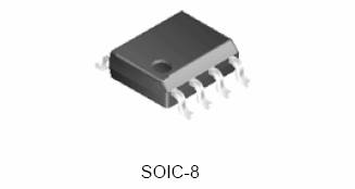 |
| Figure 1. Package Types of TD1410 |
Pin Assignments
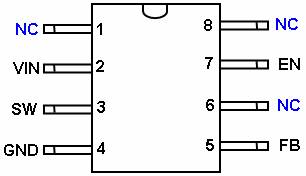 |
| Figure 2 Pin configuration of TD1410 (Top View) |
Pin Descriptions
| Pin | Name | Description |
|---|---|---|
| 1,6,8 | NC | Not Connect. |
| 2 | Vin | Supply Voltage Input Pin. TD1410 operates from a 3.6V to 20V DC voltage. Bypass Vin to GND with a suitably large capacitorto eliminate noise on the input. |
| 3 | SW | Power Switch Output Pin. SW is the switch node that supplies power to the output. |
| 4 | GND | Ground
Pin. Care must be taken in layout. This pin should be placed outside of the Schottky Diode to output capacitor ground path to prevent switching current spikes from inducing voltage noise into TD1410. |
| 5 | FB | Feedback
Pin. Through an external resistor divider network, FB senses the output voltage and regulates it. The feedback threshold voltage is 1.235V. |
| 7 | NE | Enable
Pin. EN is a digital input that turns the regulator on or off .Drive EN pin high to turn on the regulator, drive it low to turn it off. |
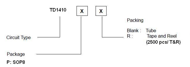
Ordering Information
Function Description
Pin Functions
+VIN
This is the positive input supply for the IC switching regulator. A suitable input bypass capacitor must be present at this pin to minimize voltage transients and to supply the switching currents needed by the regulator
GND
Circuit ground.
SW
Internal switch. The voltage at this pin switches between (VIN – VGS) and approximately – 0.5V, with a duty cycle of approximately VOUT / VIN. To minimize coupling to sensitive circuitry, the PC board copper area connected to this pin should be kept a minimum.
FB
Senses the regulated output voltage to complete the feedback loop.
EN
Allows the switching regulator circuit to be shutdown using logic level signals thus dropping the total input supply current to approximately 30uA. Pulling this pin below a threshold voltage of approximately 0.7 V turns the regulator down, and pulling this pin above 1.3V (up to a maximum of 20V) shuts the regulator on. For automatic starup condition , can be implemented by the addition of a resistive voltage divider from VIN to GND.
Functional Block Diagram
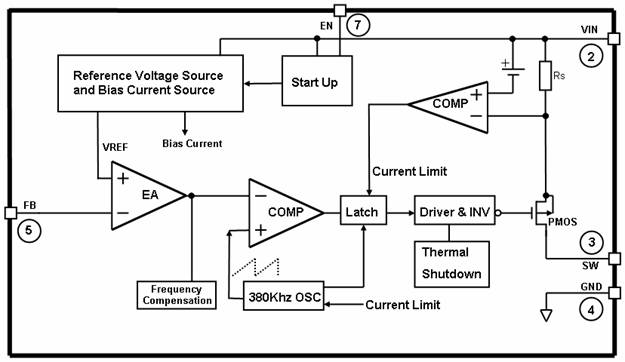
Figure 3. Functional Block Diagram of TD1410
Typical Application
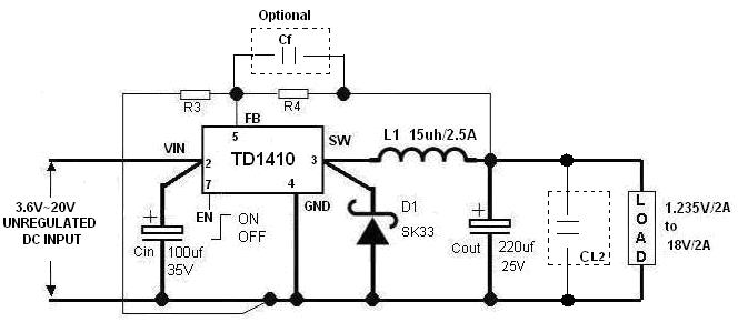
ON/OFF Controlled by external circuit
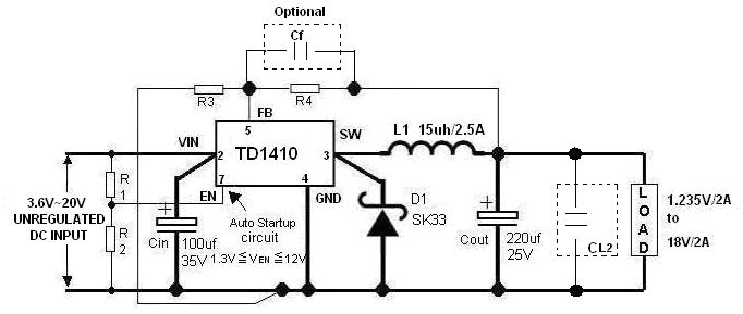
Auto-Startup Circuit
1.3V ≦ VEN=[ R2 / (R2+R1) ] *Vin < 20V (Auto-Startup)
Example : Vin=12V , Select R2=27KΩ & R1=43KΩ
→ VEN = 4.6 V (Auto-Startup)
or R2=OPEN, R1=100 KΩ When Vin < 20V (Auto-Startup)
Absolute Maximum Ratings
Note1: Stresses greater than those listed under Maximum Ratings may cause permanent damage to the device. This is a stress rating only and functional operation of the device at these or any other conditions above those indicated in the operation is not implied. Exposure to absolute maximum rating conditions for extended periods may affect reliability.
| Parameter | Symbol | Value | Unit |
|---|---|---|---|
| Input Voltage | VIN | -0.3 to 23 | V |
| Feedback Pin Voltage | VFB | -0.3 to Vin | V |
| Enable Pin Voltage | VEN | -0.3 to Vin | V |
| Switch Pin Voltage | VSW | -0.3 to Vin | V |
| Power Dissipation | PD | Internally limited | mW |
| Operating Junction Temperature | TJ | 150 | °C |
| Storage Temperature | TSTG | -65 to 150 | °C |
| Lead Temperature (Soldering, 10 sec) | TLEAD | 260 | °C |
| ESD (HBM) | 2000 | V |
Recommended Operating Conditions
| Parameter | Symbol | Min. | Max. | Unit |
|---|---|---|---|---|
| Input Voltage | VIN | 3.6 | 20 | V |
| Operating Junction Temperature | TJ | -40 | 125 | °C |
| Operating Ambient Temperature | TA | -40 | 85 | °C |
Electrical Characteristics
VCC = 12V, Ta = 25℃ unless otherwise specified.
| Parameters | Symbol | Test Condition | Min. | Typ. | Max. | Unit |
|---|---|---|---|---|---|---|
| Input voltage | VIN | 3.6 | 20 | V | ||
| Shutdown Supply Current | ISTBY | VEN=0V | 30 | 90 | uA | |
| Quiescent Supply Current | ICC | VEN=2V, VFB=1.3V | 3.6 | 4 | mA | |
| Feedback Voltage | VFB | VIN = 3.6V to 23V | 1.21 | 1.235 | 1.26 | V |
| Feedback Bias Current | IFB | VFB=1.3V | 0.1 | 0.5 | uA | |
| Switch Current Limit | ILIM | 4 | 5 | A | ||
| Oscillator Frequency | FOSC | 320 | 380 | 440 | KHz | |
| Frequency of Current Limit or Short Circuit Protection | FOSC1 | VFB=0V | 42 | KHz | ||
| EN Pin Threshold | VEN | 0.7 | 1.2 | 1.7 | V | |
| EN Pin Input Leakage Current | IH | VEN=2.5V | -0.1 | -1 | uA | |
| IL | VEN=0.5V | -3 | -10 | uA | ||
| Internal PMOS RDSON | RDSON | VIN =12V, VFB=0V | 140 | mΩ | ||
| VEN=12V, Iout=2A | ||||||
| Max. Duty Cycle | DMAX | VFB=0V, ISW=0.1A | 100 | % | ||
| Efficiency | η | Vout=5V | - | 92 | - | % |
| Iout=2A | ||||||
| Thermal Shutdown | TOTSD | 165 | °C |
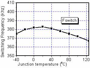
Typical Performance Characteristics
 |
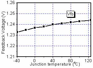 |
| Figure 5. Switching Frequency vs Temperature | Figure 6. VFB vs Temperature |
 |
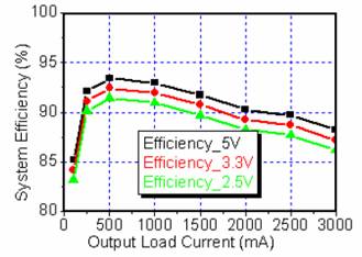 |
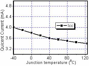
| Figure 7. Icc vs Temperature | Figure 8. Efficiency vs Load (Vin=10V) |
Typical Application Circuit
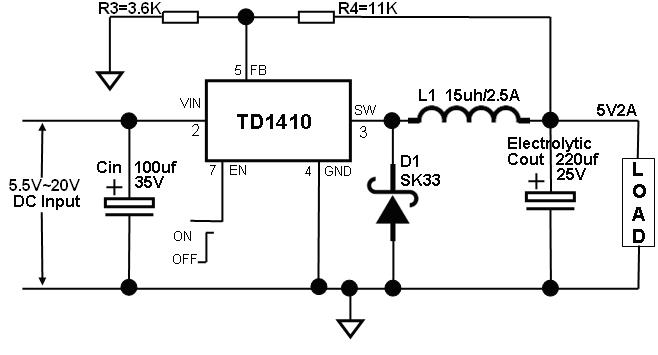
Figure 9.Typical Application Circuit@5V/2A
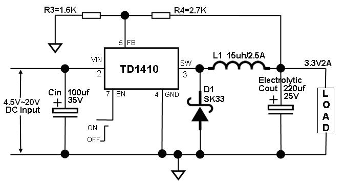
Figure 10. Typical Application Circuit@3.3V/2A
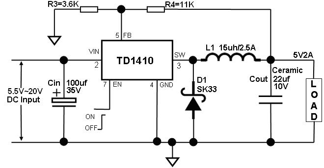
Figure 11. Typical Application Circuit@5V/2A (with ceramic output capcaitor)
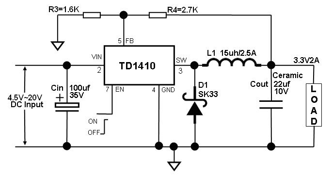
Figure 12. Typical Application Circuit@3.3V/2A (with ceramic output capcaitor)
Schottky Rectifier Selection Guide
| Vin (Max) |
2A Load Current | 3A Load Current | ||||
|---|---|---|---|---|---|---|
| Part Number | Package | Vendor | Part Number | Package | Vendor | |
| 20V | B220/A | SMB/SMA | 1 | B320/B/A | SMC/B/A | 1 |
| SS22 | SMA | 2,3 | SS32 | SMC | 2,3 | |
| MBRS320 | SMC | 4 | ||||
| SK32 | SMC | 6 | ||||
| IN5820 | D0-201AD | 6 | ||||
| 30V | B230/A | SMB | 1 | B330/B/A | SMC/B/A | 1 |
| SS23 | SMB | 2,3 | SS33 | SMC | 2,3 | |
| 20BQ030 | SMB | 4 | MBRS330 | SMC | 4,5 | |
| MBRS230 | SMB | 5 | SK33 | SMC | 3,6 | |
| SK23 | SMB | 6 | IN5821 | D0-201AD | 2,6 | |
| No. | Vendor | Web Site |
|---|---|---|
| 1 | Diodes,Inc. | www.diodes.com |
| 2 | Fairchild Semiconductor | www.fairchildsemi.com |
| 3 | General Semiconductor | www.gensemi.com |
| 4 | nternational Rectifier | www.irf.com |
| 5 | On Semiconductor | www.onsemi.com |
| 6 | Pan Jit International | www.panjit.com.tw |
Note: HY-STAR Tech provides a complete power management IC and peripheral components such as Inductors, Schottky Diode etc., please contact us if demand.
Output Voltage VS R3, R4 Resistor Selection Guide
Vout = (1+R4/R3)*1.235V
| Vout | R4 | R3 |
|---|---|---|
| 1.8V | 5.1K | 11K |
| 2.5V | 5.1K | 5K |
| 3.3V | 2.7K | 1.6K |
| 5V | 11K | 3.6K |
| 9V | 43K | 6.8K |
| 12V | 13K | 1.5K |
Termal Considerations
The TD1410 is available in SOP8 package.
The SOP8 package needs a heat sink under most conditions. The size of the heat sink depends on the input voltage, the output voltage, the load current and the ambient temperature. The TD1410 junction temperature rises above ambient temperature for a 2A load and different input and output voltages. The data for these curves was taken with the TD1410 (SOP8 package) operating as a buck-switching regulator in an ambient temperature of 25oC (still air). These temperature rise numbers are all approximate and there are many factors that can affect these temperatures. Higher ambient temperatures require more heat sinking.For the best thermal performance, wide copper traces and generous amounts of printed circuit board copper should be used in the board layout. (Once exception to this is the output (switch) pin, which should not have large areas of copper.) Large areas of copper provide the best transfer of heat (lower thermal resistance) to the surrounding air, and moving air lowers the thermal resistance even further.
Package thermal resistance and junction temperature rise numbers are all approximate, and there are many factors that will affect these numbers. Some of these factors include board size, shape, thickness, position, location, and even board temperature. Other factors are, trace width, total printed circuit copper area, copper thickness, single or double-sided, multi-layer board and the amount of solder on the board.
The effectiveness of the PC board to dissipate
heat also depends on the size, quantity and spacing of other components
on the board, as well as whether the surrounding air is still or
moving. Furthermore, some of these components such as the catch diode
will add heat to the PC board and the heat can vary as the input
voltage changes. For the inductor, depending on the physical size, type
of core material and the DC resistance, it could either act as a heat
sink taking heat away from the board, or it could add heat to the board.
Output Voltage Ripple and Transients
The output voltage of a switching power supply will contain a sawtooth ripple voltage at the switcher frequency, typically about 1% of the output voltage, and may also contain short voltage spikes at the peaks of the sawtooth waveform.
The output ripple voltage is due mainly to the inductor sawtooth ripple current multiplied by the ESR of the output capacitor.
The voltage spikes are present because of the fast switching action of the output switch, and the parasitic inductance of the output filter capacitor, To minimize these voltage spikes, special low inductance capacitors can be used, and their lead lengths must be kept short. Wiring inductance, stray capacitance, as well as the scope probe used to evaluate these transients, all contribute to the amplitude of these spikes.
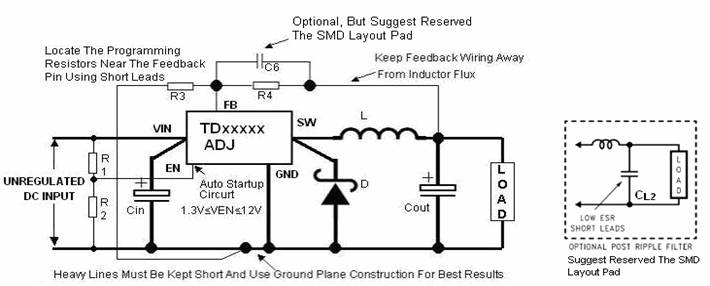
A large value inductor will also result in lower output ripple voltage , but will have a larger physical size,higher series reistance,and/or lower saturation current. An additional small LC filter can be added to the output (as shown in Figure 14) to further reduce the amount of output ripple and transients.Layout Guidelines
As in any switching regulator, layout is very important. Rapidly switching currents associated with wiring inductance can generate voltage transients which can cause problems. For minimal inductance and ground loops, the wires indicated by heavy lines should be wide printed circuit traces and should be kept as short as possible. For best results, external components should be located as close to the switcher IC as possible using ground plane construction or single point grounding.
If open core inductors are used, special care must be taken as to the location and positioning of this type of inductor. Allowing the inductor flux to intersect sensitive feedback, IC groundpath and COUT wiring can cause problems.When using the adjustable version, special care must be taken as to the location of the feedback resistors and the associated wiring. Physically locate both resistors near the IC, and route the wiring away form the inductor especially an open core type of inductor.
Figure 13, Layout Guidelines and Post Ripple Filter
Package Information
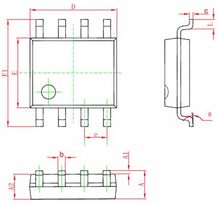
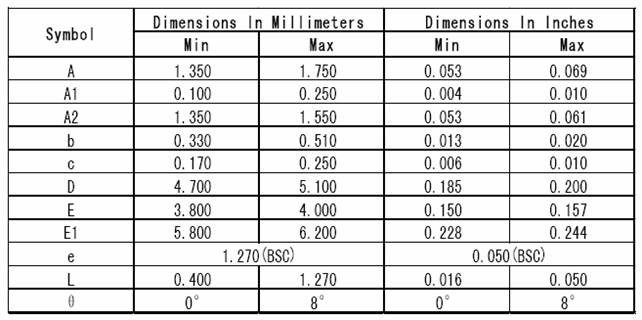
SOP8 Package Outline Dimensions
Package Information
SOP8 Carrier Tap Outline Dimensions
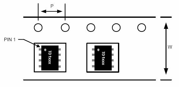
Carrier Tape, Number of Components Per Reel and Reel Size
| Package | Carrier Width (W) | Pitch (P) | Part Per Full Real | Real Size |
|---|---|---|---|---|
| SOP-8L | 12.0 ± 0.1mm | 4.0 ± 0.1mm | 2500 PCS | 330 ± 2mm |