TD1501 3A 150KHZ 45V PWM Buck DC/DC Converter
General Description
The TD1501 is a of easy to use adjustable step-down (buck) switch-mode DC/DC converter. The device is available in an adjustable or fixed output version. It is capable of driving a 3A load with excellent line and load regulation.
The output voltage is guaranteed to ±3% tolerance under specified input voltage and output load conditions. The oscillator frequency is guaranteed to ±15%.
The PWM control circuit is able to adjust the duty ratio linearly from 0 to 100%. External shutdown is included, featuring typically 80 µA standby current. Self protection features include a two stage frequency reducing current limit for the output switch and an over temperature shutdown for complete protection under fault conditions.
Requiring a minimum number of external components, these regulators are simple to use and include internal frequency compensation, and a fixed-frequency oscillator.
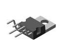
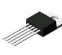
The TD1501 is available in TO-220B-5L and TO-263-5L packages.
Features
•Voltage mode non-synchronous PWM control
•Built- in switching transistor on chip
•Guaranteed 3A output load current
•Input voltage range up to 45V
•3,3V,5V and Adjustable output versions
•adjustable version output from 1.23V to 42V
•Fixed 150KHz frequency internal oscillator
•Up to 90% efficiency
•ON/OFF shutdown control input
•Low power standby mode, IQ typically 80 µA
•Thermal shutdown , current limit and short circuit protection
•Available in TO-220B and TO-263 packages
•RoHS Compliant (100% Green available)
•The minimum dropout @ Vout=5V/0.5A up to 0.9 VApplications
•Simple High-efficiency step-down regulator
•On-card switching regulators
•Positive to negative converter•LCD monitor and LCD TV
•DVD recorder and PDP TV
•Battery charger
•Step-down to 1.8/2.5/3.3/5.0 V for microprocessors
Package Types
 |
 |
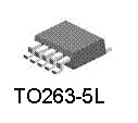 |
| TO220B-5L | TO220-5L | TO263-5L |
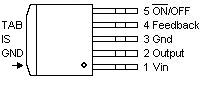
Pin Assignments
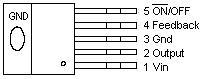 |
| TO220B-5L/TO220-5L |
 |
| TO263-5L |
Pin Descriptions
| Name | Description |
|---|---|
| Vin | Input supply voltage |
| Output | Switching output |
| Gnd | Ground |
| Feedback | Output voltage feedback input |
| ON/OFF | ON/OFF shutdown Active is“Low”or Ground |
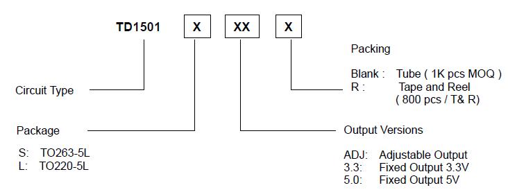
Ordering Information
Function Description
Pin Functions
+VIN
This is the positive input supply for the IC switching regulator. A suitable input bypass capacitor must be present at this pin to minimize voltage transients and to supply the switching currents needed by the regulator.GND
Circuit ground.
Output
Internal switch. The voltage at this pin switches between (+VIN – VSAT) and approximately – 0.5V, with a duty cycle of approximately VOUT / VIN. To minimize coupling to sensitive circuitry, the PC board copper area connected to this pin should be kept a minimum.Feedback
Senses the regulated output voltage to complete the feedback loop.ON/OFF
Allows the switching regulator circuit to be shutdown using logic level signals thus dropping the total input supply current to approximately 80uA. Pulling this pin below a threshold voltage of approximately 1.3V turns the regulator on, and pulling this pin above 1.3V (up to a maximum of 25V) shuts the regulator down. If thisshutdown feature is not needed, the ON /OFF pin can be wired to the ground pin or it can be left open, in either case the regulator will be in the ON condition.
Functional Block Diagram
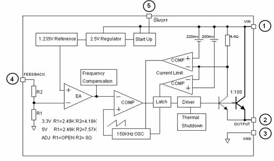
Figure 2. Functional Block Diagram of TD1501
Typical Application
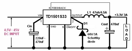
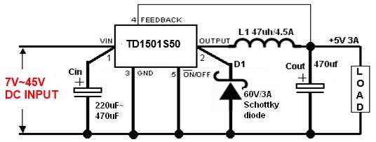
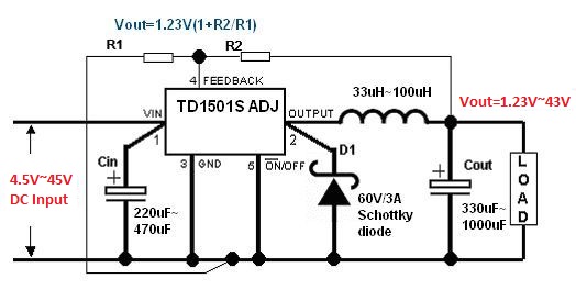
Figure 3. Typical Application of TD1501
Absolute Maximum Ratings
Note1: Stresses greater than those listed under Maximum Ratings may cause permanent damage to the device. This is a stress rating only and functional operation of the device at these or any other conditions above those indicated in the operation is not implied. Exposure to absolute maximum rating conditions for extended periods may affect reliability.| Parameter | Symbol | Value | Unit |
|---|---|---|---|
| Input Voltage | VIN | -0.3 to 45 | V |
| Feedback Pin Voltage | VFB | -0.3 to 40 | V |
| Enable Pin Voltage | Von-off | -0.3 to 25 | V |
| Output Voltage to Ground (Steady State) | VOUT | -1 | V |
| Power Dissipation | PD | Internally limited | mW |
| Operating Junction Temperature | TJ | 150 | °C |
| Storage Temperature | TSTG | -65 to 150 | °C |
| Lead Temperature (Soldering, 10 sec) | TLEAD | 260 | °C |
| ESD(HBM) | VESD | 2000 | V |
Recommended Operating Conditions
| Parameter | Symbol | Min. | Max. | Unit |
|---|---|---|---|---|
| Input Voltage | VIN | 3.6 | 45 | V |
| Operating Junction Temperature | TJ | -40 | 125 | °C |
| Operating Ambient Temperature | TA | -40 | 85 | °C |
Electrical Characteristics
(All Output Voltage Versions)Unless otherwise specified, VIN = 12V for 3.3V, 5V, adjustable version . ILOAD= 0.5A Ta = 25°C.
| Symbol | Parameter | Conditions | Min. | Typ. | Max. | Unit | ||
|---|---|---|---|---|---|---|---|---|
| VIN | Input voltage | 4.5 | 45 | V | ||||
| IQ | Quiescent current | VFB=12V force driver off | 3 | 4 | mA | |||
| IL | Output=0V | Output leakage current |
No outside circuit VFB=12V force driver off |
50 | uA | |||
| Output=-1V | VIN=40V | 2 | 30 | mA | ||||
| ISTBY | Standby quiescent current | ON/OFF pin=5V, VIN=32V | 80 | 200 | uA | |||
| Fosc | Oscillator Frequency |
125 | 150 | 170 | KHz | |||
| Fscp | Oscillator Frequency of Short Circuit Protect | When current limit occurred and VFB < 0.5V, Ta = 25℃ | 10 | 30 | 50 | KHz | ||
| VSAT | Saturation voltage |
IOUT=3A No outside circuit VFB= 0V force driver on | 1.16 | 1.4 | V | |||
| DC | Min. Dyty Cycle (ON) | VFB=12V force driver on | 100 | % | ||||
| Min. Dyty Cycle (OFF) | VFB=12V force driver off | 0 | ||||||
| VFB | Feedback Voltage | VIN= 4.5V to 45V | 1.21 | 1.235 | 1.26 | V | ||
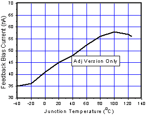
| IFB | Feedback bias current | VFB=1.3V (Adjustable version only) |
10 | 50 | nA | |||
| ICL | Current Limit | Peak Current (VFB=0V) | 3.8 |
5.5 | A | |||
| VH | ON/OFF pin logic input Threshold votage | Low (Regulaor ON) | 1.3 | 0.6 | V | |||
| VL | High (Regulator OFF) | 2.0 | 1.3 | V | ||||
| IH | ON/OFF pin logic input current | VLOGIC=2.5V(ON) | -0.01 | uA | ||||
| IL | ON/OFF pin input current | VLOGIC=0.5V(ON) | -0.1 | uA | ||||
| θJC | Thermal Resistance | TO220B-5L TO263-5L |
Junction to Case | 2.5 3.5 |
OC/W | |||
| θJA | Thermal Resistance with a copper area of approximately 3 in2 | TO220B-5L TO263-5L |
Junction to Ambient | 28 23 |
OC/W | |||
Electrical Characteristics ( Continued )
| Symbol | Parameter | Conditions | VMin | Typ. | VMAX | Unit | |
|---|---|---|---|---|---|---|---|
| TD1501 3.3 | Vout | Output Feedback | 4.75V≦VIN≦45V 0.2A≦ILOAD≦3A |
3.168 3.135 |
3.3 | 3.432 4.465 |
V |
| η | Efficiency | VIN=12V,ILOAD=3A | 73 | % | |||
| TD1501 5.0 | Vout | Output Feedback | 7V≦VIN≦45V 0.2A≦ILOAD≦3A |
4.8 4.75 |
5.0 | 5.200 5.250 |
V |
| η | Efficiency | VIN=12V,ILOAD=3A | 80 | % | |||
| TD1501 ADJ | VFB | Output Feedback | 4.5V≦VIN≦45V 0.2A≦ILOAD≦3A VOUT programmed for 3V |
1.193 1.180 |
1.23 | 1.267 1.280 |
V |
| η | Efficiency | VIN=12V,ILOAD=3A | 73 | % | |||
| TD1501 ADJ | Vout | Output Voltage | 15V≦VIN≦45V 0.2A≦ILOAD≦3A VOUT programmed for 12V |
11.52 11.4 |
12 | 12.48 12.6 |
V |
| η | Efficiency | VIN=25V,ILOAD=3A | 90 | % |
Specifications with boldface type are for full operationg temperature range, the other type are for TJ=25OC.
Typical Performance Characteristics
 |
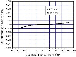 |
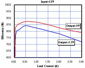
| Figure 4. Efficiency vs. Load (Vin=12V) | Figure 5. Output Voltage vs. Temperature |
 |
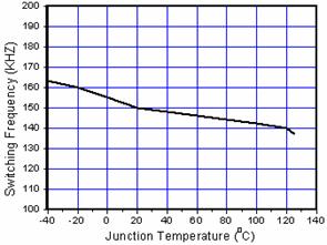 |
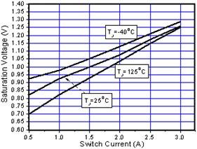
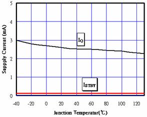
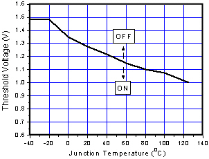
| Figure 6. Output Saturation Characteristics | Figure 7.Switching Frequency vs. Temperature |
 |
 |
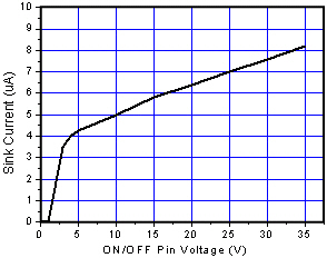
| Figure 8. Quiescent Current vs Temperature | Figure 9. ON/OFF Pin Voltage |
 |
 |
| Figure 10. ON/OFF Pin Sink Current | Figure 11. Output Saturation Characteristics |
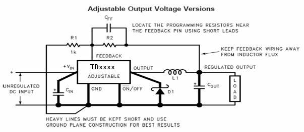
Typical Application Circuit (Adjustable
Output Voltage Version)
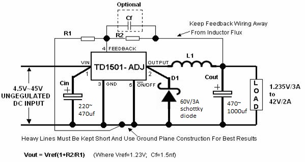
Figure 13.Typical Application of TD1501 for ADJ
| Vout | R1 | R2 | Cf(Optinal) |
3.3V |
1.6K | 2.7K | 33nf |
| 5V | 3.6K | 11K | 10nf |
| 9V | 6.8K | 43K | 1.5nf |
| 12V | 1.5K | 13K | 1nf |
Schottky Rectifier Selection Guide
| Vin (Max) |
2A Load Current | 3A Load Current | ||||
|---|---|---|---|---|---|---|
| Part Number | Package | Vendor | Part Number | Package | Vendor | |
| 20V | B220/A | SMB/SMA | 1 | B320/B/A | SMC/B/A | 1 |
| SS22 | SMA | 2,3 | SS32 | SMC | 2,3 | |
| MBRS320 | SMC | 4 | ||||
| SK32 | SMC | 6 | ||||
| IN5820 | D0-201AD | 6 | ||||
| 30V | B230/A | SMB | 1 | B330/B/A | SMC/B/A | 1 |
| SS23 | SMB | 2,3 | SS33 | SMC | 2,3 | |
| 20BQ030 | SMB | 4 | MBRS330 | SMC | 4,5 | |
| MBRS230 | SMB | 5 | SK33 | SMC | 3,6 | |
| SK23 | SMB | 6 | IN5821 | D0-201AD | 2,6 | |
| 40V | B240/A | SMB/SMA | 1 | B340/B/A | SMC/B/A | 1 |
| SS24 | SMB | 1,3,5 | SS34 | SMC | 2,3 | |
| MBRS240 | SMB | 5 | Q0BQ040 | SMC | 4 | |
| MBRS340TR | SMC | 4,5 | ||||
| SK34 | SMC | 6 | ||||
| IN5822 | D0-201AD | 6 | ||||
| 50V | B250 A | SMB/SMA | 1 | B350/B/A | SMC/B/A | 1 |
| SS25 | SMB | 2,3 | SS35 | SMC | 2,3 | |
| SK23 | SMB | 5 | MBRS330 | SMC | 4,5 | |
| SK35 | SMC | 3.6 | ||||
| Vin (Max) |
4A Load Current | 5A Load Current | ||||
|---|---|---|---|---|---|---|
| Part Number | Package | Vendor | Part Number | Package | Vendor | |
| 20v | SL42 | SMC | 2,3 | B520C | SMC | 1 |
| SR502 | DO-201AD | 1 | ||||
| SB520 | DO-201AD | 2 | ||||
| IN5823 | DO-201AD | 6 | ||||
| 30V | SL43 | SMC | 2,3 | B530C | SMC | 1 |
| SR503 | DO-201AD | 1 | ||||
| SB530 | DO-201AD | 2 | ||||
| SSC53L | SMC | 3 | ||||
| IN5824 | D0-201AD | 6 | ||||
| 40V | SL44 | SMC | 2,3,5 | B540C | SMC | 1 |
| SR504 | DO-201AD | 1 | ||||
| SB540 | DO-201AD | 2 | ||||
| SSC54 | SMC | 3 | ||||
| IMBRS540T3 | SMC | 5 | ||||
| IN5825 | DC-201AD | 6 | ||||
| 50V | B550C | DC-201AD | 6 | |||
| SB550 | SMC | 1 | ||||
| DC-201AD | 2 | |||||
Application Hints and Layout Guidelines
Heat Sink / Thermal Considerations
The TD1501 is available in two packages, a 5-pin TO-220B/TO220 and a 5-pin surface mount TO-263.The TO-220B/TO220 package needs a heat sink under most conditions. The size of the heatsink depends on the input voltage, the output voltage, the load current and the ambient temperature. The TD1501 junction temperature rises above ambient temperature for a 3A load and different input and output voltages. The data for these curves was taken with the TD1501 (TO-220B/TO220 package) operating as a buck switching regulator in an ambient temperature of 25oC (still air). These temperature rise numbers are all approximate and there are many factors that can affect these temperatures. Higher ambient temperatures require more heat sinking.
The TO-263 surface mount package tab is designed to be soldered to the copper on a printed circuit board. The copper and the board are the heat sink for this package and the other heat producing components, such as the catch diode and inductor. The PC board copper area that the package is soldered to should be at least 0.4 in2, and ideally should have 2 or more square inches of 2 oz. Additional copper area improves the thermal characteristics, but with copper areas greater than approximately 6 in2, only small improvements in heat dissipation are realized. If further thermal improvements are needed, double sided, multilayer PC board with large copper areas and/or airflow are recommended.
The TD1501 (TO-263 package) junction temperature rise above ambient temperature with a 3A load for various input and output voltages. This data was taken with the circuit operating as a buck switching regulator with all components mounted on a PC board to simulate the junction temperature under actual operating conditions. This curve can be used for a quick check for the approximate junction temperature for various conditions, but be aware that there are many factors that can affect the junction temperature. When load currents higher than 3A are used, double sided or multilayer PC boards with large copper areas and/or airflow might be needed, especially for high ambient temperatures and high output voltages.
For the best thermal performance, wide copper traces and generous amounts of printed circuit board copper should be used in the board layout. (Once exception to this is the output (switch) pin, which should not have large areas of copper.) Large areas of copper provide the best transfer of heat (lower thermal resistance) to the surrounding air, and moving air lowers the thermal resistance even further.Output Voltage Ripple and Transients
The output voltage of a switching power supply will contain a sawtooth ripple voltage at the switcher frequency, typically about 1% of the output voltage, and may also contain short voltage spikes at the peaks of the sawtooth waveform.
The output ripple voltage is due mainly to the inductor sawtooth ripple current multiplied by the ESR of the output capacitor.
The voltage spikes are present because of the fast switching action of the output switch, and the parasitic inductance of the output filter capacitor, To minimize these voltage spikes, special low inductance capacitors can be used, and their lead lengths must be kept short. Wiring inductance, stray capacitance, as well as the scope probe used to evaluate these transients, all contribute to the amplitude of these spikes.
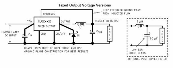
A large value inductor will also result in lower output ripple voltage , but will have a larger physical size,higher series reistance,and/or lower saturation current. An additional small LC filter can be added to the output (as shown in Figure 14) to further reduce the amount of output ripple and transients.Layout Guidelines
As in any switching regulator, layout is very important. Rapidly switching currents associated with wiring inductance can generate voltage transients which can cause problems. For minimal inductance and ground loops, the wires indicated by heavy lines should be wide printed circuit traces and should be kept as short as possible. For best results, external components should be located as close to the switcher IC as possible using ground plane construction or single point grounding.
If open core inductors are used, special care must be taken as to the location and positioning of this type of inductor. Allowing the inductor flux to intersect sensitive feedback, IC groundpath and COUT wiring can cause problems.When using the adjustable version, special care must be taken as to the location of the feedback resistors and the associated wiring. Physically locate both resistors near the IC, and route the wiring away form the inductor especially an open core type of inductor.
Figure 14, Layout Guidelines and Post Ripple Filter
Package Information (TO220B-5L)
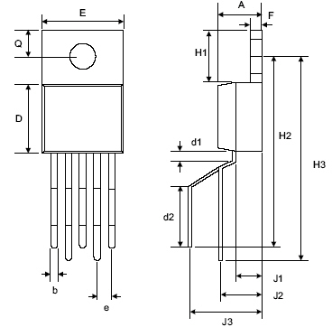
| Symbol | Dimensions In Millimeters | Dimensions In Inches | ||
|---|---|---|---|---|
| Min. | Max. | Min. | Max. | |
| A | 0.44 | 0.47 | 0.175 | 0.185 |
| b | 0.07 | 0.09 | 0.027 | 0.037 |
| D | 0.84 | 0.89 | 0.33 | 0.35 |
| d1 | 0.1 | 0.039 | ||
| d2 | 0.63 | 0.248 | ||
| E | 9.91 | 10.41 | 0.39 | 0.41 |
| e | 0.16 | 0.18 | 0.062 | 0.072 |
| F | 0.12 | 0.13 | 0.048 | 0.052 |
| H1 | 0.64 | 0.25 | ||
| H2 | 2.08 | 2.24 | 0.82 | 0.88 |
| H3 | 2.39 | 2.55 | 0.942 | 1.002 |
| J1 | 0.27 | 0.105 | ||
| J2 | 0.37 | 0.53 | 0.147 | 0.207 |
| J3 | 0.84 | 0.331 | ||
| Q | 0.25 | 0.3 | 0.1 | 0.12 |
Package Information(TO220-5L)
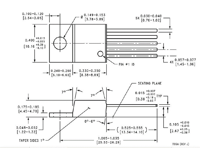
Package Information (TO263-5L)
| Symbol | Dimensions In Millimeters | Dimensions In Inches | ||
|---|---|---|---|---|
| Min. | Max. | Min. | Max. | |
| A | 4.06 | 4.83 | 0.16 | 0.19 |
| B | 0.76 | 1.02 | 0.03 | 0.04 |
| C | 0.36 | 0.64 | 0.014 | 0.025 |
| C2 | 1.14 | 1.4 | 0.045 | 0.055 |
| D | 8.64 | 9.65 | 0.34 | 0.38 |
| E | 9.78 | 10.54 | 0.385 | 0.415 |
| e | 1.57 | 1.85 | 0.062 | 0.073 |
| F | 6.6 | 7.11 | 0.26 | 0.28 |
| L | 15.11 | 15.37 | 0.595 | 0.605 |
| L2 | - | 1.4 | - | 0.055 |
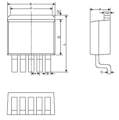
Packing Information
TO263-5L Carrier Tape Outline Dimensions
Carrier Tape, Number of Components Per Reel and Reel Size
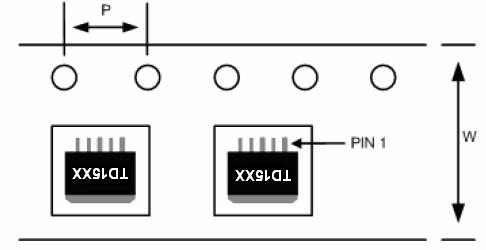
| Package | Carrier Width (W) | Pitch (P) | Part Per Full Real | Real Size |
|---|---|---|---|---|
| TO263-5L | 24.0 ± 0.1mm | 4.0 ± 0.1mm | 800 PCS | 330 ± 2mm |